4 layer Flex PCB Manufacturing and Stackup guidelines
4 layer flex PCB are used in a variety of industrial applications. Our flex PCBs are first choice for industries such as power, automobile, medical devices, GPS, and industrial control equipment, to name a few.
Four Layer Flex PCB Stack up
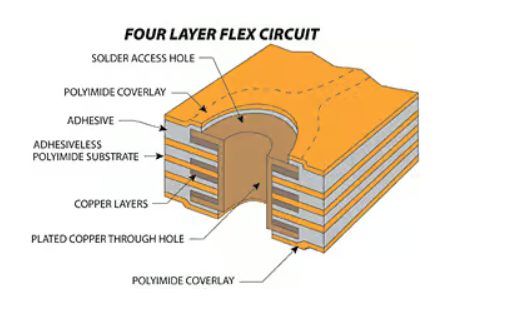
Flexible printed circuits (FPCs) provide invaluable dynamic flexing and shape conforming capabilities in electronics. 4 layer flex PCBs with conductors on 4 layers enable increased routing density and integration versus 2 layer flex, while retaining excellent flexibility.
This article examines 4 layer flex stackup configurations, critical design guidelines, the manufacturing challenges involved, advanced capabilities needed for quality 4 layer FPCs, and techniques for optimizing performance.
What is a 4 Layer Flex PCB?
A 4 layer flex PCB consists of:
- Flexible base dielectric material such as polyimide forming the core.
- Copper foil conductors patterned on the top, bottom and two inner layers of the core.
- Cover layers laminated above and below for insulation, abrasion resistance and stiffness.
- Plated through holes (PTH) and buried vias for vertical interconnections.
- Edge contacts or stiffeners to provide external connections.
This construction provides the highest routing density on a flex PCB with fine conductors and clearances.
Applications of 4 Layer Flex Circuits
Some common applications leveraging 4 layer flex PCB technology include:
- Wearable devices – Smart watches, fitness trackers, AR/VR headsets.
- Flexible displays – Edge or foldable displays, large LED video walls.
- Automotive – In-car displays, lane departure systems, LiDAR.
- Aerospace/Military – Helmet systems, communications, guidance systems.
- Medical – Ultrasound transducers, implants, endoscopes.
- Industrial – Flexible HMIs, robotic interconnects, motion control.
- Consumer Electronics – Foldable phones, cameras, portable electronics.
The ultra-dense interconnect capabilities of 4 layer FPCs supports the complex, compact and lightweight requirements of these applications.
Benefits of 4 Layer Flexible PCBs
Some key advantages of 4 layer flex PCBs are:
- Maximum routing density – Complex, compact layouts with traces on 4 layers.
- Embedded discrete passives – Buried resistor, capacitor and inductor integration.
- Controlled impedances – Tight impedance control for matched high speed signals.
- Integrated shielding – Entire layers can provide EMI/RFI isolation.
- Higher component density – More components in a given area with multilayer escape routing.
- Multilayer stacking – Can integrate other flex or rigid-flex layers.
- Greater functionality – High density interconnects enable more capabilities and features.
- Miniaturization – Ideal for complex circuits in small, lightweight products.
- Lower assembly costs – Eliminates separate flexible cabling and connectors.
- High frequency performance – Controlled impedances benefit RF applications.
4 Layer Flex PCB Stackup Configurations
Common 4 layer flex stackup arrangements include:
Symmetrical Arrangement
Coverlayer Signal Layer 1
Ground Plane Signal Layer 2 Flexible Core Dielectric Signal Layer 3 Ground Plane Signal Layer 4 Coverlayer
This offers good EMI control with ground plane shielding and similar layer structures on both sides of the core.
Asymmetrical Arrangement
Coverlayer Signal Layer 1 Ground Plane 1 Power Layer
Flexible Core Dielectric Signal Layer 2 Ground Plane 2 Signal Layer 3 Coverlayer
Here power and ground planes are distributed on each side of the core dielectric to provide isolation between signals.
High Speed Arrangement
Coverlayer Signal Layer 1 Ground Plane 1 Signal Layer 2 Flexible Core Dielectric Signal Layer 3 Signal Layer 4 Ground Plane 2 Coverlayer
Fast signals demanding impedance control are assigned to the outer layers in this configuration. Power and ground planes provide constant reference planes.
Challenges in 4 Layer Flex PCB Fabrication
While delivering substantial benefits, producing 4 layer flex PCBs poses difficulties:
- Achieving fine lines and spaces on multiple flexible layers.
- Holding tight layer-to-layer registration through all photolithography stages.
- Producing high density of buried and blind microvias with thin dielectric.
- Preventing lifted lands or cracked barrel plating on PTHs during flexing.
- Maintaining reliable coverlayer and stiffener adhesion through dynamic flexing.
- Controlling characteristic impedances across multiple flex layers.
- Managing thermomechanical stresses and fatigue prone areas.
- Qualification testing of impedance shifts under long term flex cycling.
- Ensuring flex fold and bend cycle life reaches millions of cycles.
Advanced Manufacturing Capabilities Required
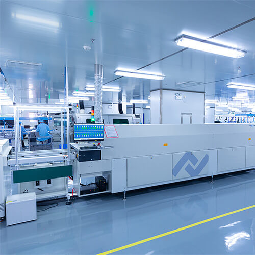
To reliably fabricate 4 layer flex circuits, PCB manufacturers need substantial expertise:
- Fine line etching – Trace/space widths down to 25μm on multilayer flex materials.
- Registration accuracy – Alignment of +/- 50μm between flexible layers.
- Microvia construction – Laser drilled and plated blind/buried vias with 1:1 capture pads.
- ANNULAR ring control – Producing 1 mil rings reliably on buried microvias.
- Multilayer bonding – Interlayer peel strength over 2.5N/mm without delamination.
- Surface finish – Immersion silver with thickness uniformity of <10% across flex contours.
- Impedance tolerance – Tight impedance control within 5% of target value.
- Flexible solder mask – Liquid photoimageable (LPI) solder mask optimized for flexing.
- Reliability testing – Extreme temperature cycling, twisting, bending, vibration and drop testing.
- Process Control – Real-time statistical process monitoring and control.
- Flex fold engineering – Precisely defined and characterized bend radiuses backed by extensive test data.
4 Layer Flex Design Recommendations
Some key guidelines when designing 4 layer flex PCBs:
- Plan stackup arrangement to isolate critical signals using ground planes.
- Use impedance matched traces with adequate shielding for high speed signals.
- Model impedances and performance under dynamic bending conditions.
- Widen trace/space dimensions in flexing areas relative to rigid sections.
- Incorporate strain relief structures at interfaces between rigid and flex sections.
- Utilize thermal reliefs for solder joints to reduce stresses.
- Add stiffeners or covers for rigidity at connection points.
- Maximize distance of components from high flex zones.
- Define and specify multiple controlled bend radii rather than arbitrary flexing.
- Review layouts for susceptibility to acid traps during fabrication.
- Specify microvia capture pads with 1:1 aspect ratio for reliability.
- Consider needs for shielding, insulation and abrasion resistance in stackup design.
Conclusion
4 layer flex PCB technology enables innovative products with maximum routing density combined with dynamic flexing capabilities. To harness these benefits requires proper stackup configurations, controlled processes, and sound flex design techniques. Partnering with an expert flex PCB manufacturer having robust 4 layer technology maturity allows designers to fully leverage the advantages of 4 layer flex to develop cutting-edge solutions for flex electronics integration needs across industries.


