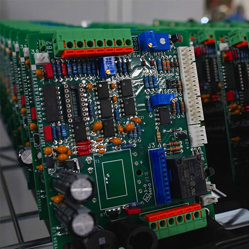
What is the Difference Between 2 Layers and 4 Layers PCB Costs
2 layer and 4 layer PCBs are two of the most commonly used PCB types in technology. There are many other options regarding PCB layers, such as one, 04 layers to 6 or 8 layers PCBA. But 2-layer and 4-layer PCBAs are widely used in most prototype or technical devices because of their ease of installation.
In addition, its simple design and high cost-performance ratio are also prominent factors in its popularity. In this article, we will compare these two PCB components and explain their features and cost factors one by one.
2-layer PCB
2-layer PCBs may be very cost-effective, lightweight, and simple, but they may not be suitable for various devices that require more delicate signals to provide the required results. We will see its advantages and disadvantages here:
Advantages
The most important point is that the cost of 2-layer PCBs is lower than that of 4-layer designs.
Its design and production are simple, and you can get your printed circuit board faster. The simpler your plan, the less likely you are to make costly mistakes during the design or manufacturing process.
If you need a large number of PCBAs, you should choose double-layer because it is cost-effective and requires less time.
You can develop a 2-layer PCBA in a shorter time, so you don’t have to wait too long.
Disadvantages
More components can be used in a 4-layer PCB compared to a 2-layer PCB.
It is slow. So if speed is an issue, the more layers the better. Depending on the application, you may find that two layers are not enough to provide the necessary speed and capacity for your project.
Although 4-layer printed circuit boards have more layers, double-sided PCBs are usually quite large and bulky compared to leaving space for components and leads.
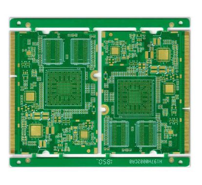
4-layer PCBs
4-layer PCBAs have their own advantages and disadvantages, mainly the following:
Advantages
It is useful for more complex projects. The more complex your project is, the more valuable you will find the additional layers of a 4-layer PCB.
It provides you with high quality. Going from 2-layer to 4-layer PCB design is an obvious choice for even simple products that require the highest quality.
It can handle more power, which is a considerable advantage for 4-layer PCBs. When deciding whether you need a double-sided or 4-layer PCB, consider how much energy your design requires.
Compared to 2-layer PCBs, 4-layer designs are more durable due to the higher number of layers
Disadvantages
Since 4-layer PCBs use more materials and are more challenging to manufacture, the cost of 4-layer PCBs can be much higher than 2-layer PCBs.
Due to the increasing number of layers involved, the design will also become more complex, and it will take time to develop such a design.
Due to the complexity of the design, few manufacturers in the market are able to provide such components.
Making 4-layer PCBAs is a time-consuming process.
Its repair is more complicated, and double-sided PCBs have an advantage over four-layer designs in terms of ease of repair.
Comparing 2-layer and 4-layer PCBs based on stackup
2-layer PCB stackup
Due to the simplicity of design, 2-layer PCBs are relatively easy to limit or develop. The topmost layer is called layer 1 and is made of copper material. You can customize the thickness of this layer according to your design.
4-layer PCB Stackup
A 4-layer PCB has an FR4 core or glass core with two prepreg sheets bonded lengthwise on both sides. All 4 layers of PCBA are connected by soldering at the joints.
These interconnections are on the outermost and outermost copper layers. Also, the design or stackup of a 4-layer PCB is more complex than a 2-layer PCB.
Comparison of 2 Layers and 4 Layers PCB based on their respective designs
2-layer PCB Design
In a two-layer PCB design, more surface area is available for conductor layout. A two-layer PCB has twice the surface area of a single-layer PCB. Vias route the traces to the other side of the PCB. Hence, all connections are made through vias.
4-layer PCB Design
A four-layer PCB has a larger surface area than a two-layer design. When designing a four-layer PCB, planning is more complex than a two-layer board. Heat and pressure are required to bond the prepreg between the top and lower outer layers.
It is easy to determine the number of layers of a PCB by counting the number of different conductor designs. The number of conductor designs matches the number of PCB layers. A typical 4-layer PCB design has four different conductor layouts that are easy to identify.
Functionality of 2-layer and 4-layer PCBs
In terms of functionality, 2-layer PCBs have no propagation delay. Since there are fewer layers to deal with, it is easier to construct microstrip traces on the ground plane. The functionality of 4-layer PCBs may be affected by impedance issues or propagation delays due to increased signal complexity.
Therefore, 4-layer PCBs can be used in systems where signal delay is not a significant issue. Since the ground layer, VCC, and two signal layers on these boards provide insulation and heat resistance, they are also suitable for equipment that is used for a long time.
Cost Comparison of 2-layer and 4-layer PCBs
The cost of 2-layer PCBs is lower due to the simplicity of design. The design of 4-layer PCBs is more complex. A higher degree of skill and experience is required to complete this design. Therefore, the design cost of 4-layer PCBs is higher than that of 2-layer PCBs.
In addition to reducing distortion and improving propagation levels, the complex architecture of 4-layer PCBs enables it to achieve these goals. 4-layer PCBs cost more because it provides better performance by improving signal integrity and reducing interference to zero.
Developers are willing to spend more for 4-layer PCBs because it makes it simpler to get superior features in their products; they prefer it over 2-layer PCBs.
Prototyping with 2-layer and 4-layer PCBs: Performance Difference
Manual prototyping is a thing of the past. Prototyping with 2-layer and 4-layer PCBs can be done quickly and simply with tools such as Gerber. Building a 4-layer PCB is no more difficult than making a 2-layer PCB because you just add extra layers.
The complexity of the design does not make prototyping more difficult because it almost makes it an automated process, removing the work from the development phase of the product.
Outsourcing PCB prototyping is a common practice for most companies. When it comes to creating prototypes, these professionals have a set of ready-made systems. To ensure that your PCB prototype is produced on time and without errors, it is best to hire a professional PCB designer who has experience in similar projects.
The prototyping services provided by the experts use custom design tools. In addition, they have running production lines, online quotation systems that respond immediately, and the ability to submit Gerber files quickly.
Due to these features, prototyping issues are no longer a concern for PCB designers. Therefore, both 2-layer and 4-layer PCBs are equally suitable for prototyping.
2-layer vs 4-layer Comparison Points
When deciding whether to choose a 2-layer or 4-layer PCB, there are a few things to consider. So, take a look at whether a 2-layer or 4-layer PCB solution is the best for your application:
The internal components of the device must be as small as possible to maximize functionality within a limited space. This is a 4-layer PCB, which is smaller in size but more powerful. Therefore, a 4-layer PCB is more suitable for manufacturing small and feature-rich devices.
Devices with more complex functions may benefit from a 4-layer PCB, which is a good fit for such devices. Therefore, for gadgets that require unique operations, 4-layer PCBs are the best solution.
4-layer PCBs are great for gadgets because they can improve durability. Although 4-layer PCBs cost more, they have a longer shelf life. They can continue to operate like brand new due to the sturdy operation of 4-layer PCBs.
2-layer PCBs may be more effective than single-layer PCBs for controlling device costs. Low-cost electronics may benefit from 2-layer PCBs because 2-layer PCBs cost less.
If you need to create a device quickly, 2-layer PCBs can help you meet deadlines. 5. 2-layer PCBs are a better solution for device production due to simpler designs.
In addition, when making a decision, you need to check the required operating frequency, signal flow design, and density. Due to these factors, it is necessary to compare two-layer PCBs and four-layer PCBs.
2-layer and 4-layer PCBs differ in design complexity. In addition, the thickness and time required for development are also different. 2-layer PCBs cost less than 4-layer PCBAs because they are less complex and require no materials. Therefore, 4-layer PCBs cost more.
Nevertheless, 4-layer PCBs are still a better choice because they are more powerful. They perform equally well in the prototyping process thanks to software and professional design services.

